Bridges and PCI Internal works
Introduction
Have you ever thought how device memory mapping work internally? This article is going to explain peripheral devices internal since I've been asked couple of time to explain how peripheral devices works and are communicated with processors, for example, LPC controller, SCSI controller, LAN controller.Physical Memory partitioning by Host Bridge / NorthBridge
As we all known, There's two way to communicate between processor to PCI devices(in PCI speaking master-slave) , I/O port access or Memory mapped access.For memory mapped access, for the same address, for example - 0xA1000, how hardware distinguish that's for devices, and isn't for system memory access? The secret is hidden by host bridge memory partitioning.
In Host bridge / North Bridge, there's memory controller, and graphic controller and the root complex logic that connects to SouthBridge / PCH by Direct Media Interface (DMI) , to handle all device communication from processor. As following example Intel x99 chipset architecture
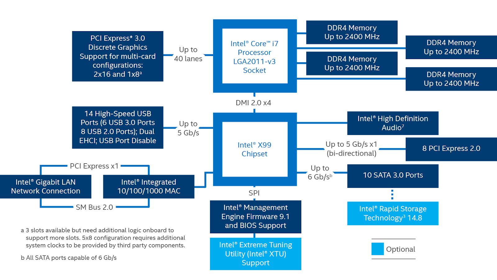 |
| Figure [1] |
But the question is how the Host bridge distinguish where to dispatch each memory access, i.e. To System Memory or transfer the request to PCI devices? and how avoid OS or Software misuses the physical memory region to prevent fatal mistake as these regions should be reserved by devices or vice versa?
There's some hints can be found from Host Bridge's physical memory partitioning configuration, it divided system memory into several regions, OS visible memory, PCI device memory and even some other reserved usage, which is internally implemented by its address decoder on address bus, and which make the host root complex logic is able to confidently direct the request to the right place, i.e. (Main Memory vs PCI Device)
As an example for physical memory partitioning.
 |
| Figure [2] |
PCI Device Memory Space Configuration
The base address of PCI device memory region can be configured by both TOLUD (Top of Low Usable DRAM) and TOUUD (Top of Upper Usable DRAM) register which is stored in Host Bridge (B0:D0:F0) PCI configuration space and offset is corresponding to the processor family. These registers indicate where should PCI device memory space start in terms of lower and upper region.(less than 4 GB and more than 4 GB PCI Device Address Space respectively) |
| Figure [3] |
 |
| Figure [4] |
How the device memory to be routed to the target device?
So, Now, Host Bridge takes advantages from these configuration to identify when and where to route the memory access, however, there's next question is that the Host Bridge is not going to do further partition for the specific usage of its PCI address space for devices, so how PCI bus is able to direct and start the transaction to the PCI devices and get the job done?Base Address Register (BAR)
There's two set of BAR (either 6 BAR in 32 bit or 3 BAR in 64 bit addressing) which depends on the device, BAR is stored in PCI configuration space, and it always point to the PCI device memory space, it is assigned by BIOS or UEFI to reserve memory regions, BAR also determines the way (I/O or Memory) how processor can communicate with itself. As following structure bit 0 is always 0. It can be different in terms of device.
| 31 - 4 | 3 | 2 - 1 | 0 |
|---|---|---|---|
| 16-Byte Aligned Base Address | Prefetchable | Type | Always 0 |
| 31 - 2 | 1 | 0 |
|---|---|---|
| 4-Byte Aligned Base Address | Reserved | Always 1 |
PCI Signals
 |
| Figure [5] |
AD# - PCI transaction consist one destination address and one or more return data
FRAME# - initiate the transaction request
DEVSEL# - Assert when a PCI device accept transaction and start to return data in AD pins
IDRY# - Write data is valid and ready, device reading the data from AD pins
TDRY# - Read data is valid and ready, device writing the data into AD pins
Request PCI Device to Start Transaction
After the memory request has been identified by Host Bridge that will be delivered to the South Bridge to process further PCI transaction, PCI processing will be started by asserting AD# , C/BE#, FRAME# pins in order.The memory address and operation will be filled in AD pins (AD[63:0] pins for 64 bit addressing or AD[31:0] pins for 32 bit addressing) and C/BE pins in each PCI devices, and eventually assert FRAME# signal to tell the device, "you are good to go ". Simplify logic as following digram.
 |
| Figure [6] |
Respond to PCI bus's transaction request
At any given time, all devices will have a chance to accept and respond to each requests theoretically, however, in the cycle of address phase, devices have to determine if the incoming physical memory address is included in their BAR or desired memory location like BIOS reset vector for SPI controller it then asserts Device Select Signal - DEVSEL# in three cycle to begin the transaction and start to process the transaction data to/from on the BAR space during the rest of cycles in AD pin until FRAME# pin is return to the unassertive state. In chipset speaking, we called this kind of decoding to Positive Decoding - Devices knows what is their desired memory location. |
| Figure [7] |
Positive Decoding vs. Subtractive Decoding
There's two method that PCI device can be choose to decode the incoming transaction, positive decoding or subtractive decoding, mostly it will be the first case, however, for the bridge type PCI device it used to subtractively decode the transaction so the the transaction can be reached as much PCI device endpoint as possible.Positive decoding is when a device claim the transaction because of the requested memory address is fall into the device's desired memory address space, e.g. within its BAR, as opposed to it is Subtractive Decoding, device claims the transaction whenever there's no any devices claim the transaction on the same PCI bus, regardless of the device is desired the address or not, as mentioned, it's used to be used by bridge type device.
PCI device memory access is always subtractively decoded by DMI interface controller in Host Bridge, which means, it will be claimed by DMI interface controller to send the transaction to lower level - the PCH / South Bridge if there's no device that claims the transaction in the Host Bridge's PCI device tree, and it will be the most cases.
 |
| Figure [8] |
The other example of it is PCI-to-PCI Bridge device, that claims decode the transaction subtractively

Comments
Post a Comment